What Is SMT? An Engineering-Level Guide to Surface Mount Technology
Surface Mount Technology (SMT) is the backbone of modern electronics manufacturing.
From smartphones and automotive electronics to industrial control systems and medical devices, SMT enables high-density, high-reliability PCB assembly at scale.
However, SMT is often misunderstood as simply “placing and soldering components.”
In reality, it is a system-level manufacturing discipline that integrates materials science, precision equi
pment, thermal control, automation, software, and reliability engineering.
This article provides a practical, engineering-oriented overview of SMT, covering its fundamentals,
evolution, completeprocess flow, and future trends—based on real production experience.
1. What Is Surface Mount Technology (SMT)?
SMT is an electronic assembly technology in which surface-mou
nt devices (SMDs)—components with no leads or very short leads—are mounted directly onto the surface of a printed circuit board (PCB).
Compared with traditional Through-Hole Technology (THT), SMT offers clear advantages:
Higher component density
Better suitability for automation
Lower overall manufacturing cost
Improved electrical performance for high-speed and high-frequency designs
Today, SMT is the default assembly method for most electronic products.
Core Elements of SMT
SMT consists of three tightly connected elements:
1. Surface-Mount Components (SMD/SMC)
Common packages include 0201, 0402, QFP, BGA, CSP, and MELF.
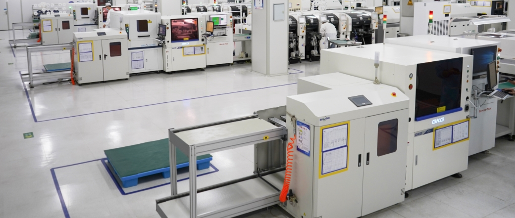
2. SMT Equipment
Solder paste printers
Pick-and-place machines
Reflow ovens
Inspection systems (SPI, AOI, AXI)
3. SMT Process Flow
Solder Paste Printing → Component Placement → Reflow Soldering → Inspection → Rework
Engineering Insight:
SMT performance depends less on individual machines and more on process stability and coordination across the entire production line.
2. The Evolution of SMT
SMT has evolved continuously alongside component miniaturization and manufacturing automation:
1960s – Planar packaging concepts introduced
1970s – Mass production of chip resistors and capacitors
1980s – Global packaging standards established (JEDEC, IEC)
1990s – High-speed placement machines and BGA packaging
2000s – 01005 components, CSP, and flip-chip technologies
2010s – SiP, PoP, and module-level assembly
2020s – Industry 4.0, AI-driven inspection, and smart factories
Each stage reflects the same industry drivers: smaller components, higher accuracy, and greater reliability.
3. Complete SMT Process Flow (Double-Sided Reflow Example)
1. Incoming Quality Control (IQC)
All PCBs, components, and solder materials are inspected for:
RoHS compliance
Moisture Sensitivity Level (MSL)
Coplanarity and solderability
Tools may include 3D X-ray inspection, solderability testing, and cross-section analysis.
2. PCB Baking
Purpose: Remove absorbed moisture to prevent delamination or cracking during reflow.
Typical parameters:
125 °C for 4–8 hours
OSP boards: lower temperature and shorter time (e.g. 105 °C for 2 hours)
3. Solder Paste Printing
Using fully automatic stencil printers (e.g. DEK, EKRA, MPM), key parameters include:
Stencil thickness: 0.10–0.15 mm
Aperture ratio: 0.8–1.0 × pad area
Printing speed: 25–100 mm/s
SPI systems monitor paste height, volume, and alignment.
Engineering Insight:
In real production, printing consistency is one of the most critical factors affecting SMT yield.
4. Adhesive Dispensing (Optional)
Applied in double-sided reflow when heavy components are mounted on the bottom side.
Glue volume: 0.0003–0.001 g per dot
Curing: thermal or UV
5. Component Placement
High-speed and flexible placement machines are used depending on component type.
Typical performance:
Accuracy: ±15–25 µm (3σ)
Speed: over 100,000 CPH for small passive components
Key controls include vacuum pickup force, vision alignment, and placement pressure.
6. Reflow Soldering
Multi-zone forced convection reflow ovens are used, often with nitrogen protection.
Typical profile:
Ramp-up: 1–3 °C/s
Soak: 60–120 s
Peak temperature: 235–245 °C
Controlled cooling: 3–6 °C/s
Engineering Insight:
Reflow quality depends on the balance between time above liquidus (TAL), flux activation, and thermal uniformity, not peak temperature alone.

7. Post-Reflow Cleaning (Optional)
Required for high-reliability applications such as automotive and medical electronics.
Standard: IPC-CH-65B
Ionic contamination ≤ 1.56 µg NaCl/cm²
8. Inspection (AOI & AXI)
AOI detects missing parts, polarity issues, solder bridges, and tombstoning
AXI is essential for BGA, QFN, and other hidden solder joints
3D inspection and AI-based algorithms are increasingly used to reduce false calls.
9. Functional Testing (FCT)
Includes ICT testing, system-level functional tests, and boundary scan (JTAG) for complex ICs.
10. Rework and Reliability Validation
Defective assemblies are repaired using BGA rework stations or laser-assisted systems.
Reliability tests may include:
Thermal cycling
Vibration and mechanical stress
Cross-section and dye penetration analysis
4. Future Trends in SMT
Ultra-miniaturization: 008004 components entering mass production
Advanced packaging: SiP, Chiplet, Fan-Out RDL
Green manufacturing: low-void, low-temperature soldering materials
Smart factories: digital twins, predictive maintenance, MES–ERP integration
Flexible electronics: FPC and roll-to-roll SMT processes
Conclusion
SMT has evolved into a highly integrated manufacturing system rather than a simple assembly process.
For manufacturers and suppliers alike, mastering SMT means understanding the interaction between materials, equipment, process parameters, and long-term reliability.
As electronic products continue to demand higher density and reliability, SMT remains a critical foundation of modern electronics manufacturing.
Add comment